|

  
LM / CD 74LS00 series TTL IC's: 7451 / 74LS51 to 7497 / 74LS97 series
  

These "LS" chips are basically low power drain CMOS versions of the TTL range.
Please note, we do not stock all the listed chips on this page, however we can
order these in, depending on availability, "lead" times. These useful 74LSxxx building
blocks of logic IC's function are on lower voltages, eg: typically from 4.5V ~ 5.6V D.C.
Email us :sales@unitechelectronics.com
    7451
  2-wide 2-input and 2-wide 3-input AND-NOR gates.
      +---+--+---+                  _____________________
   1A |1  +--+ 14| VCC        /1Y = (1A.1B.1C)+(1D.1E.1F)
   2A |2       13| 1B
   2B |3       12| 1C               _______________
   2C |4  7451 11| 1D         /2Y = (2A.2B)+(2C.2D)
   2D |5       10| 1E
  /2Y |6        9| 1F
  GND |7        8| /1Y
      +----------+
    7454
  4-wide 2/3-input AND-NOR gate.
      +---+--+---+                 ___________________________
    A |1  +--+ 14| VCC        /Y = (A.B)+(C.D.E)+(F.G.H)+(J.K)
    B |2       13| K
    C |3       12| J
    D |4  7454 11| H
    E |5       10| G
   /Y |6        9| F
  GND |7        8|
      +----------+
 
    7455
  2-wide 4-input AND-NOR gate.
      +---+--+---+                 ___________________
    A |1  +--+ 14| VCC        /Y = (A.B.C.D)+(E.F.G.H)
    B |2       13| H
    C |3       12| G
    D |4  7455 11| F
      |5       10| E
      |6        9|
  GND |7        8| /Y
      +----------+
    7457
  Frequency divider.

  This device can generate a one second timing pulses from 60 Hertz.
  Two 7457 devices may be inter-connected to give frequency division
  of 3,600 to 1, 1,800 to 1, 900 to 1, etc. This chip is unique in
  that it features a reset pin that is common to all 3 counters.
       +---+--+---+
  CLKB |1  +--+  8| QC
   VCC |2        7| QB
    QA |3  7457  6| RST
   GND |4        5| CLKA
       +----------+
    7458
  2-wide 2-input and 2-wide 3-input AND-OR gates.

      +---+--+---+
   1A |1  +--+ 14| VCC         1Y = (1A.1B.1C)+(1D.1E.1F)
   2A |2       13| 1B
   2B |3       12| 1C
   2C |4  7458 11| 1D          2Y = (2A.2B)+(2C.2D)
   2D |5       10| 1E
   2Y |6        9| 1F
  GND |7        8| 1Y
      +----------+
7472
and-gated J-K master-slave flip-flops with preset and clear/reset.
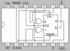
+---+--+---+ +--------+--------+---+----+----*---+---+
|1 +--+ 14| VCC |J1.J2.J3|K1.K2.K3|CLK|/SET|/RST| Q |/Q |
/RST |2 13| /SET +========+========+===+====+====*===+===+
J1 |3 12| CLK | X | X | X | 0 | 0 | ? | ? |
J2 |4 7472 11| K3 | X | X | X | 0 | 1 | 1 | 0 |
J3 |5 10| K2 | X | X | X | 1 | 0 | 0 | 1 |
/Q |6 9| K1 | 0 | 0 | / | 1 | 1 | - | - |
GND |7 8| Q | 0 | 1 | / | 1 | 1 | 0 | 1 |
+----------+ | 1 | 0 | / | 1 | 1 | 1 | 0 |
| 1 | 1 | / | 1 | 1 |/Q | Q |
| X | X |!/ | 1 | 1 | - | - |
+--------+--------+---+----+----*---+---+
    7473
  Dual negative-edge-triggered J-K flip-flop with reset.
  Please Note: The supply VCC is pin 4, Gnd is pin 11.


        +---+--+---+           +---+---+----+----*---+---+
  /1CLK |1  +--+ 14| 1J        | J | K |/CLK|/RST| Q |/Q |
  /1RST |2       13| /1Q       +===+===+====+====*===+===+
     1K |3       12| 1Q        | X | X |  X |  0 | 0 | 1 |
    VCC |4  7473 11| GND       | 0 | 0 |  \ |  1 | - | - |
  /2CLK |5       10| 2K        | 0 | 1 |  \ |  1 | 0 | 1 |
  /2RST |6        9| 2Q        | 1 | 0 |  \ |  1 | 1 | 0 |
     2J |7        8| /2Q       | 1 | 1 |  \ |  1 |/Q | Q |
        +----------+           | X | X | !\ |  1 | - | - |
                               +---+---+----+----*---+---+
    7474
  Dual D flip-flop with set and reset.
        +---+--+---+           +---+---+----+----*---+---+
  /1RST |1  +--+ 14| VCC       | D |CLK|/SET|/RST| Q |/Q |
     1D |2       13| /2RST     +===+===+====+====*===+===+
   1CLK |3       12| 2D        | X | X |  0 |  0 | 1 | 1 |
  /1SET |4  7474 11| 2CLK      | X | X |  0 |  1 | 1 | 0 |
     1Q |5       10| /2SET     | X | X |  1 |  0 | 0 | 1 |
    /1Q |6        9| 2Q        | 0 | / |  1 |  1 | 0 | 1 |
    GND |7        8| /2Q       | 1 | / |  1 |  1 | 1 | 1 |
        +----------+           | X |!/ |  1 |  1 | - | - |
                               +---+---+----+----*---+---+
    7475
  Dual 2-bit transparent latches with complementary outputs.
  Please Note:The supply VCC is pin 5, Gnd is pin 12.
       +---+--+---+
  /1Q1 |1  +--+ 16| 1Q1
   1D1 |2       15| 1Q2
   1D2 |3       14| /1Q2
   2LE |4       13| 1LE
   VCC |5  7475 12| GND
   2D1 |6       11| /2Q1
   2D2 |7       10| 2Q1
  /2Q2 |8        9| 2Q2
       +----------+
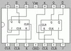
    7476
  Dual J-K flip-flops with set and reset.
  Please Note: The supply VCC is pin 5, Gnd is pin 13.
        +---+--+---+           +---+---+---+----+----*---+---+
   1CLK |1  +--+ 16| 1K        | J | K |CLK|/SET|/RST| Q |/Q |
  /1SET |2       15| 1Q        +===+===+===+====+====*===+===+
  /1RST |3       14| /1Q       | X | X | X |  0 |  0 | 0 | 0 |
     1J |4       13| GND       | X | X | X |  0 |  1 | 1 | 0 |
    VCC |5  7476 12| 2K        | X | X | X |  1 |  0 | 0 | 1 |
   2CLK |6       11| 2Q        | 0 | 0 | / |  1 |  1 | - | - |
  /2SET |7       10| /2Q       | 0 | 1 | / |  1 |  1 | 0 | 1 |
  /2RST |8        9| 2J        | 1 | 0 | / |  1 |  1 | 1 | 0 |
        +----------+           | 1 | 1 | / |  1 |  1 |/Q | Q |
                               | X | X |!/ |  1 |  1 | - | - |
                               +---+---+---+----+----*---+---+
    7478
  Dual negative-edge-triggered J-K flip-flops with common clock,
  set and common reset.
  Please Note: The supply VCC is pin 4, Gnd is pin 11.
        +---+--+---+           +---+---+----+----+----*---+---+
   /CLK |1  +--+ 14| 1K        | J | K |/CLK|/SET|/RST| Q |/Q |
  /1SET |2       13| 1Q        +===+===+====+====+====*===+===+
     1J |3       12| /1Q       | X | X |  X |  0 |  0 | ? | ? |
    VCC |4  7478 11| GND       | X | X |  X |  0 |  1 | 1 | 0 |
   /RST |5       10| 2J        | X | X |  X |  1 |  0 | 0 | 1 |
  /2SET |6        9| /2Q       | 0 | 0 |  \ |  1 |  1 | - | - |
     2K |7        8| 2Q        | 0 | 1 |  \ |  1 |  1 | 0 | 1 |
        +----------+           | 1 | 0 |  \ |  1 |  1 | 1 | 0 |
                               | 1 | 1 |  \ |  1 |  1 |/Q | Q |
                               | X | X | !\ |  1 |  1 | - | - |
                               +---+---+----+----+----*---+---+
    7483
  4-bit binary full adder with fast carry.
  Please Note: The supply VCC is pin 5, Gnd is pin 12.
      +---+--+---+
   A4 |1  +--+ 16| B4          S=A+B+CIN
   S3 |2       15| S4
   A3 |3       14| COUT
   B3 |4       13| CIN
  VCC |5  7483 12| GND
   S2 |6       11| B1
   B2 |7       10| A1
   A2 |8        9| S1
      +----------+
    7485
  4-bit noninverting magnitude comparator with cascade inputs.
       +---+--+---+
    B3 |1  +--+ 16| VCC
  IA<B |2       15| A3
  IA=B |3       14| B2
  IA>B |4       13| A2
  OA>B |5  7485 12| A1
  OA=B |6       11| B1
  OA<B |7       10| A0
   GND |8        9| B0
       +----------+
    7486
  Quad 2-input XOR gates.
      +---+--+---+             +---+---*---+                    _   _
   1A |1  +--+ 14| VCC         | A | B | Y |       Y = A+B = (A.B)+(A.B)
   1B |2       13| 4B          +===+===*===+
   1Y |3       12| 4A          | 0 | 0 | 0 |
   2A |4  7486 11| 4Y          | 0 | 1 | 1 |
   2B |5       10| 3B          | 1 | 0 | 1 |
   2Y |6        9| 3A          | 1 | 1 | 0 |
  GND |7        8| 3Y          +---+---*---+
      +----------+
    7490
  4-bit asynchronous decade counter with /2 and /5 sections, set(9) and reset.
  Please Note: The supply VCC is pin 5, Gnd is pin 10.
        +---+--+---+
  /CLK1 |1  +--+ 14| /CLK0
   RST1 |2       13|
   RST2 |3       12| Q0
        |4  7490 11| Q3
    VCC |5       10| GND
   SET1 |6        9| Q1
   SET2 |7        8| Q2
        +----------+
    7491
  8-bit serial-in serial-out shift register with two
  AND gated serial inputs and complementary outputs.
  Please Note: the supply VCC is on pin 5, Gnd is pin 10.
      +---+--+---+
      |1  +--+ 14| /Q7
      |2       13| Q7
      |3       12| D
      |4  7491 11| E
  VCC |5       10| GND
      |6        9| CLK
      |7        8|
      +----------+
    7492
  4-bit asynchronous divide-by-twelve counter with /2 and /6 sections and reset.
  Please Note: the supply VCC is on pin 5, Gnd is pin 10.
        +---+--+---+
  /CLK1 |1  +--+ 14| /CLK0
        |2       13|
        |3       12| Q0
        |4  7492 11| Q3
    VCC |5       10| GND
   RST1 |6        9| Q1
   RST2 |7        8| Q2
        +----------+
    7493
  4-bit asynchronous binary counter with /2 and /8 sections and reset.
  Please Note: The supply Vcc is on pin 5, Gnd is pin 10.
        +---+--+---+
  /CLK1 |1  +--+ 14| /CLK0
   RST1 |2       13|
   RST2 |3       12| Q0
        |4  7493 11| Q3
    VCC |5       10| GND
        |6        9| Q1
        |7        8| Q2
        +----------+
    7495
  4-bit universal shift register with separate shift and parallel-load clocks.
         +---+--+---+
       D |1  +--+ 14| VCC
      P0 |2       13| Q0
      P1 |3       12| Q1
      P2 |4  7495 11| Q2
      P3 |5       10| Q3
  LD//SH |6        9| SHCLK
     GND |7        8| LDCLK
         +----------+
    7496
  5-bit shift register with asynchronous reset and asynchronous preset inputs.

      +---+--+---+
  CLK |1  +--+ 16| /RST
   P0 |2       15| Q0
   P1 |3       14| Q1
   P2 |4       13| Q2
  VCC |5  7496 12| GND
   P3 |6       11| Q3
   P4 |7       10| Q4
   PE |8        9| D
      +----------+
    7497
  6-bit synchronous binary rate multiplier.
  Can perform fixed-rate or variable-rate frequency division.
  Output frequency is equal to input frequency multiplied by
  the rate input M and divided by 64.
        +---+--+---+
     B1 |1  +--+ 16| VCC
     B4 |2       15| B3
     B5 |3       14| B2
     B0 |4       13| RST
      Z |5  7497 12| U/CAS
      Y |6       11| ENin
  ENout |7       10| STRB
    GND |8        9| CLK
        +----------+
" DISCLAIMER "
We believe the above information to be correct, however,  typographical errors
can occur and it is for this very reason, we provide the above information "as is"
with "no Warranty" as to "correctness" nor to its "accuracy". Please, always
check  with your " own data books "  or via a "Google" search on the net.
Please notify us if you have discovered a typographical error and we will fix it.
 E. &. O. E.
This page was upgraded January 30th 2013
|