These "LS" chips are basically low power drain CMOS versions of the TTL range.
Please note, we do not stock all the listed chips on this page, however we can
order these in, depending on availability, "lead" times. These useful 74LSxxx building
blocks of logic IC's function are on lower voltages, eg: typically from 4.5V ~ 5.6V D.C.


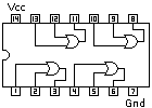
 +---+--+---+ +---+---+---*---+ ___
1A |1 +--+ 14| VCC | A | B | C |/Y | /Y = ABC
1B |2 13| 1C +===+===+===*===+
2A |3 12| /1Y | 0 | X | X | 1 |
2B |4 7410 11| 3C | 1 | 0 | X | 1 |
2C |5 10| 3B | 1 | 1 | 0 | 1 |
/2Y |6 9| 3A | 1 | 1 | 1 | 0 |
GND |7 8| /3Y +---+---+---*---+
+----------+
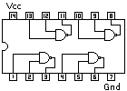
+---+--+---+ +---+---+---*---+ ___
1A |1 +--+ 14| VCC | A | B | C |/Y | /Y = ABC
1B |2 13| 1C +===+===+===*===+
2A |3 12| /1Y | 0 | X | X | 1 |
2B |4 7410 11| 3C | 1 | 0 | X | 1 |
2C |5 10| 3B | 1 | 1 | 0 | 1 |
/2Y |6 9| 3A | 1 | 1 | 1 | 0 |
GND |7 8| /3Y +---+---+---*---+
+----------+
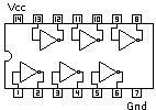
 +---+--+---+ ________
A |1 +--+ 14| VCC /Y = ABCDEFGH
B |2 13|
C |3 12| H
D |4 7430 11| G
E |5 10|
F |6 9|
GND |7 8| /Y
+----------+
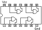
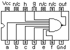
+---+--+---+ ________
A |1 +--+ 14| VCC /Y = ABCDEFGH
B |2 13|
C |3 12| H
D |4 7430 11| G
E |5 10|
F |6 9|
GND |7 8| /Y
+----------+